
Producing 1 PCB is very different from producing many PCBs, especially considering the logistics of assembling and testing. In this blog post, we'll continue the story from last time and look at the revised versions and how to scale up the production with PCB assembly and a test jig.
Testing and review
The initial revision of the PCB worked for the most part. All the critical sensors appeared to be working, but we found a few things to improve on the design, and a design review with James Munns helped identifying some additional improvements.
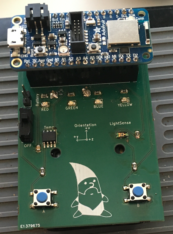
Button placement
The button placement was too close to the thumb when operating with one hand. The fix for this was to place them closer to the center.
LED brightness
The LEDs functioned correctly, but the brightness was not completely even. In particular, the red and green LEDs were a lot brighter than the others. After doubling the resistance, the brightness of the LEDs were a lot more balanced.
Battery measurement
The battery measurement circuit was wrong, and caused inputs outside the ADC range of the microcontroller. Fixing this involved using different resistor values for the circuit.
Accelerometer orientation
In order to make the sensor output compatible with both the Adafruit Feather nRF52840 Sense and Feather Adafruit nRF52840 Express, we switched the orientation of the accelerometer to make sure the output axes values was the same.
Board outline
The sharp edges are a bit annoying when using the device. Given that this device is supposed to be used in a game like setting, we added some rounded corners.
In addition,we added a few holes so that we could add a string and users would be able to wear the device around their neck.
To avoid any potential for radio interference of the Adafruit from the PCB, we also added a keep out zone beneath the radio for good measure.
Power
In the initial revision, the power switch was connected to the EN pin of the Adafruit, as this would allow us to use the switch for LiPoly batteries as well. However, even in this mode the device draws power, so we decided to have the switch control the battery power source directly and remove the jumper pins we placed there to prevent accidental reverse current. Instead, we added a Schottky diode to prevent the case of reverse current with both batteries and USB power connected.
Pairing with BLE Mesh
Since the devices are going to be part of a BLE Mesh network and paired with a single application, we need a way to provision them and identify them. In order to do that, we decided to make room for a QR code sticker in the middle of the board. Then, upon flashing the device, we would set the expected mesh node UUID in the device firmware, and create a mapping between the UUID and a QR code.
The pairing process will then use this data to ensure sensor data is routed to the expected application.
Wiring and traces
In the initial revision, the outline made no use of ground vias, a technique that adds vias to the board in order to reduce the path from components to ground.
New revision
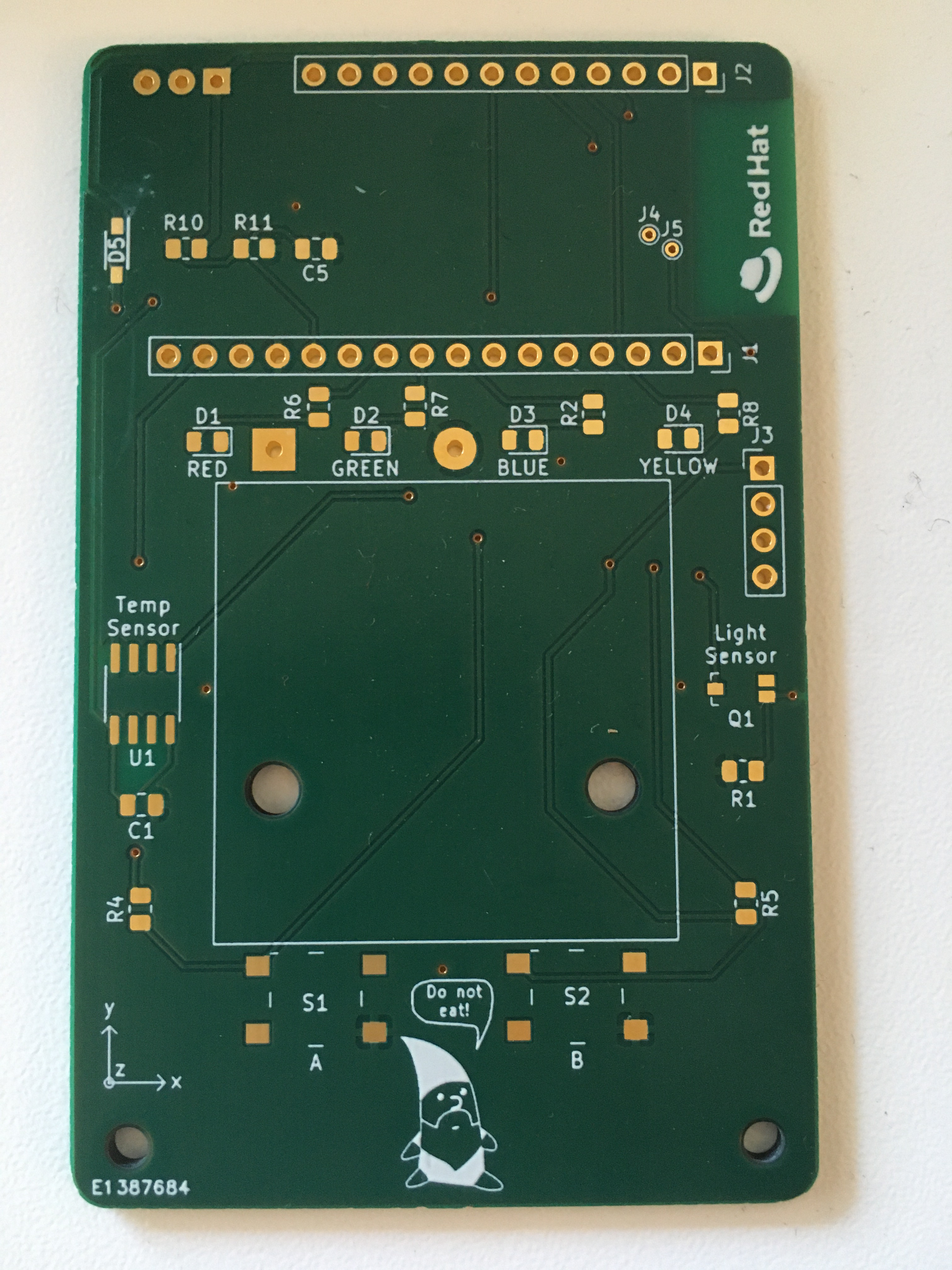
Having fixed the defects, we also initially removed the accelerometer footprint from the PCB, and revision 3.0 did not include it
Revision 3.0 felt much better in hand, and all sensors worked as we hoped. The biggest unknown before testing was the Schottky diode (which is a component we had not tested before)
as you can see below. However, to avoid risking supply chain issues, we quickly decided to add it back for a final revision 3.5, with the option of not soldering it when scaling up production.
Flash jig
Programming the Adafruit Feather nRF52840 Express/Sense without the builtin bootloader requires powering the device from USB and attaching an external programmer using one of the following alternatives:
- Attaching a SWD cable (only available on the Express)
- Solder wires to SWD solder pads on the back side of the feather
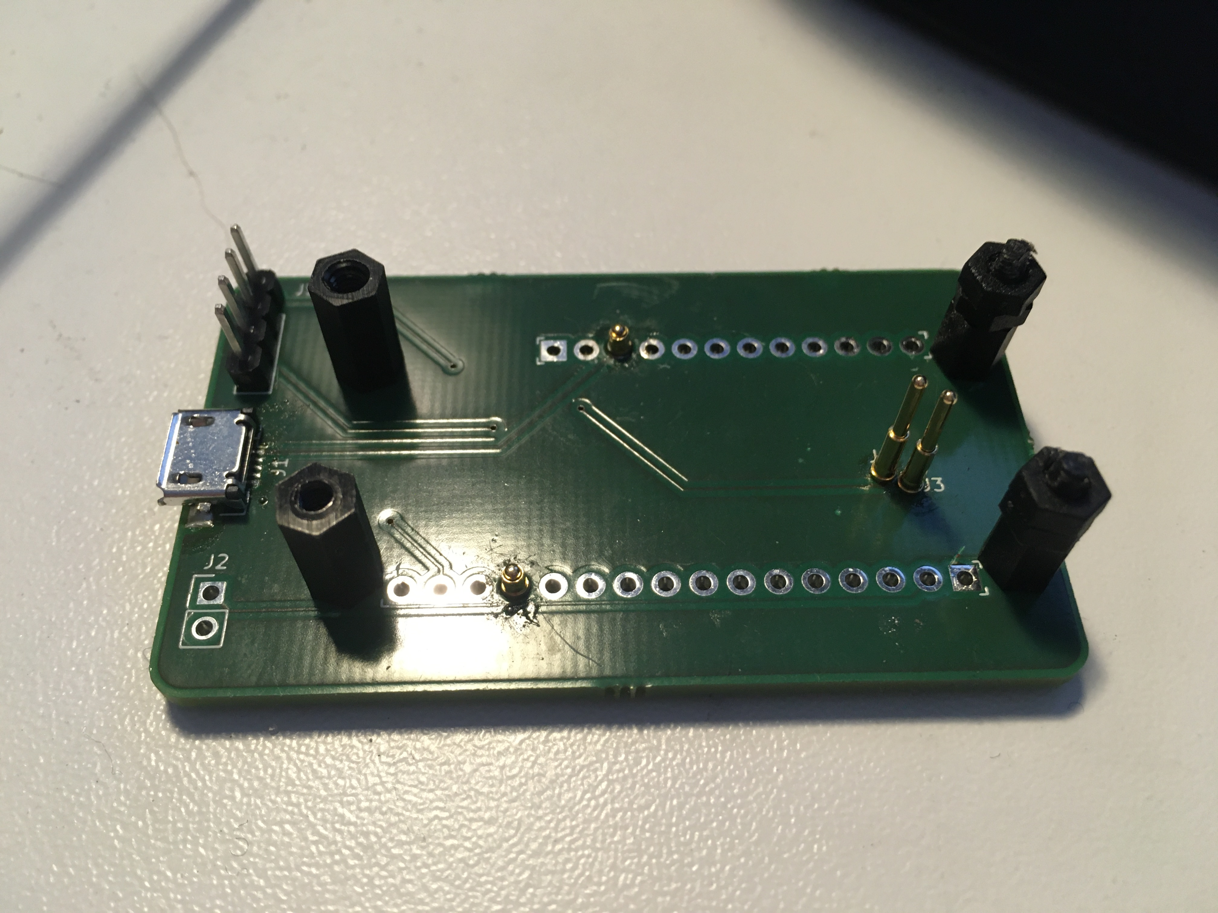
Both alternatives work for a few devices, but with the potential of 500 devices being made, we needed a better and more efficient way to program them. After reading about test jigs, we decided to build a custom test jig for the feather, with the goal of not needing any connectors to be attached in order to program the feather.
In order to do that, we did research on the use of spring loaded pins, aka pogo pins. After initial experimentation to understand how these pins behaved, we ended up with a setup that worked quite well, and would allow us to spend most time only waiting for the flash operation to succeed.
In order to build the jig, we needed another custom PCB which had the appropriate footprints for the pogo pins, as well as a way to power the feather using the VUSB and GND pins. After some trial and error, we found some pins that worked out nicely with the feather pins. The board draws power from USB, which will also power the feather when pressed down on the jig. The debug probe is connected to the 4 pins (VTarget, SWDIO, SWDCLK, GND). When the feather touches the standoffs, it will touch all 4 pogo pins as well, at which point one can program the device with the debug probe.
We also published a video of how to operate the test jig with one hand.
PCB assembly
For someone not familiar with PCB manufacturing, getting to the point where we could order fully assembled devices was a challenge. Most manufacturers have some online quotation service, but ultimately it was easier talking to their sales department and get the necessary help. We decided to order 5 fully assembled PCBs from RushPCB, who were very helpful and guiding us to retrieve the information they needed.
For the assembly, we had to prepare (in addition to the gerbers for PCB production itself):
- A Bill of Materials (BOM) for all the components, including the manufacturing part number and the reference designator on the board where it should be placed.
- A component placement file, which can be prepared by KiCad.
- Assembly drawings and instructions. This is essentially a document containing the silk screen, fabrication outline and drill layers, with comments if you have any special requirements. The important part here is that you should assume this document to be read by a human being if clarifications are needed.
Before scaling up production, we decided to order 5 initial pre-assembled boards from RushPCB to ensure we got things right.
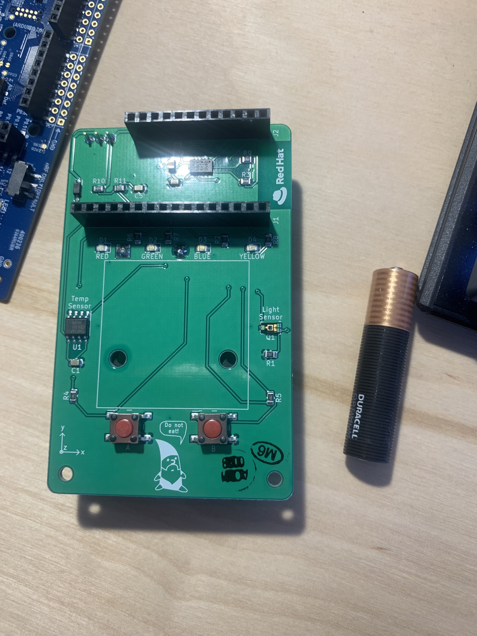
The final revision worked as we hoped, with some tweaks to ensure the firmware were using the correct ports. After spending some time with the accelerometer, we also made some improvements for the driver to work reliably.
Summary
Throughout these two blog posts, we've seen the steps we took starting from the initial drawing to a potential large scale manufacturing of a fully assembled PCB, including additional equipment to program the devices. A lot of trial and error is expected when trying something new, but we got something that worked in the end. With KiCad, there is a lot of open hardware
All the design for the PCB can be found on github. You can also find the firmware that runs the BLE Mesh and BLE GATT services, and early stages of a GATT client/gateway and BLE Mesh gateway, which we'll write more about in the future.
Eventually, the large scale manufacturing of this device did not happen, but we certainly learned a lot in the process, which we plan to make use of as we want to create more boards to demonstrate Drogue IoT, both cloud and device.